Editors’ Picks


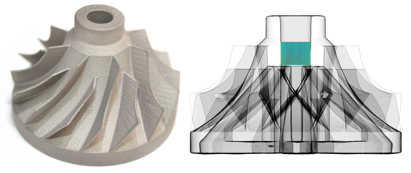
Decades ago, the world of diagnostic single-exposure X-rays was supplemented with the layer-by-layer, 3D density details generated by microscale X-ray computed tomography (microCT) imaging. Just as engineers have long used standard X-rays to examine the internal structure of traditionally manufactured parts, developers and quality assurance groups have more recently applied the deeper capabilities of microCT to parts produced by additive manufacturing (AM). One of the many benefits of metal AM is the ability to produce internal structures. Parts must not only meet dimensional specs but also display consistent and acceptable quality characteristics, such as high density and the absence of…
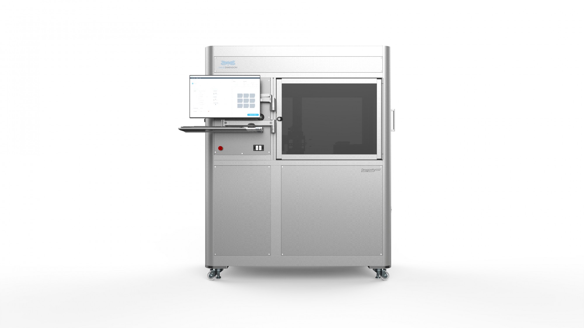
If you’ve been following the development of additive manufacturing (AM) systems focused on the electronics industry, you’ve heard about Nano Dimension. In 2012, the company began developing its dual-material DragonFly system for 3D-printing prototype multi-layer printed circuit boards (PCBs). The approach combines inkjet technology with 3D printing using proprietary nanotechnology-based conductive and dielectric inks. Users are able to produce their own complex, high quality prototype PCBs in hours instead of days or weeks (the usual turn-around time for out-sourced boards). 3D-printed multilayer PCB. Top layer displays traces with various trace- and space-widths, as well as non-plated and plated through-holes and…


